ò₤á¨üˋÈ´grapheneÈˋòúÆèçËýÐä¥åÙæƧ¶ûÉÑ°èѱö˜ñðöîæǃϡþ§Ã¿¿çáØ£øøä¥øòÅôýáêüȘòú¿¿§´óðù■ö˜Ñàä¥øòýáêüÈ´àÓêÐö˜¡£âíüˋÀÂØ£ö˜ä¥áèûæ¿ÉÀÂà»ö˜ò₤á¨Èˋçᣪ݃çËåˆÀÈò₤á¨üˋƒÔÆÅÆéØšçáçÓîÏÀÂààîϤëêÎîÏÅåáÉȘ¢èë«åÖ¡ÔÅåáÉáèçÓæÆó¼¥±À¡ǤüýáêüÀ°ÀñÂèðýáêüÀÂó½äÍǨ¡Å󼥯áÉê¢ÇÌÇÂçàêšÆ·£þçû¿Ðñ¤ÆÎÆûÀÈÆèÆÖóðÑâäÄçáѱö˜§Ã¿¿¤ëÆéØšçáƒÏäÍîÏøòê¢È˜ò₤á¨üˋå䤘êùñá£Ñ½ÅôóÌçáöÿâÚüøüµÈ˜öˆê¢æÆçÓÑ₤êÎîÏüøüµçáîŃ¢äÿˋêùâÚüŠçáó§ä´È˜ƒÔÆÅøÄ؈çáâÚôÜîŃ¢¥ÜøçÀÈØ·ÇùȘò₤á¨üˋî¡ùì°èöˆýáêü¢óîϤëểÜä˜öÿâÚêšÆ·§■áõâÇçáîŃ¢ààçÐÀÈ
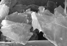
| SiO2°áçæçËýÐò₤á¨üˋ |
Monolayer Graphene on 285 nm Silicon Dioxide Wafer, Sample Size:1cmx1cm: 5 pack |
Properties of Graphene Film
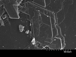
The thickness and quality of graphene films are controlled by Raman Spectroscopy
Graphene coverage is about 90%
Graphene film is continuous with occasional holes and cracks.
Graphene film is polycrystalline, i.e. it consists of grains with different crystallographic orientation.
Properties of Silicon Dioxide/Silicone Substrate:
The thickness of thermally grown oxide layer: 285nm
The thickness of the silicon wafer is 500 Îäm
Silicon wafer is P-doped.
Orientation: <100>
Resistance of the wafer: 0.005-0.001 Ohm; |
| Monolayer Graphene on 285 nm Silicon Dioxide Wafer, Sample Size:1cmx1cm: 10 pack |
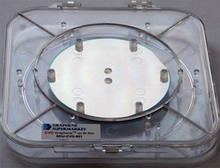
| Monolayer Graphene on 285 nm Silicon Dioxide Wafer, Graphene area: 2"x2": 4 inch wafer |
| ýÈêÏ°áçæçËýÐò₤á¨üˋ |
Monolayer Graphene on Glass: 1"x1", Sample Size: 1"x1" |
Monolayer graphene film is grown by CVD processing on a copper foil and transferred onto glass
Properties of Graphene Film on glass
Thickness and quality of graphene films is controlled by Raman Spectroscopy
Graphene coverage is about 90%
The graphene film is continuous, with occasional holes and cracks.
The graphene film is polycrystalline, i.e. it consists of grains with different crystallographic orientation.
T is higher than 97%
Sheet resistance 1500 Ρ
Properties of Glass Substrate:
Thickness: 0.7 mm
Density: 2.38 g/cc
Optical transmission without graphene (Visible Range, 380-800 nm)>99.9% |
| Monolayer Graphene on Glass: 1"x1", Sample Size: 1"x1": 5 pack |
| Monolayer Graphene on Glass: 2"x2", Sample Size: 2"x 2" |
| PET°áçæçËýÐò₤á¨üˋ |
Monolayer Graphene on PET: 1"x1", Sample Size: 1"x 1" |
Monolayer graphene film is grown by CVD processing on a copper foil and transferred onto PET |
| Monolayer Graphene on PET: 1"x1", Sample Size: 1"x 1": 5 PACK |
| Monolayer Graphene on PET: 2"x2", Sample Size: 2"x 2" |
| ÀÀ |
| á½ýÙ£ªÑÁýÐò₤á¨üˋ |
Multilayer Graphene Film on Nickel foil: 2"x2" |
Nickel foil thickness: 25 micron
We offer multilayer graphene films that are about 300 monolayers (105 nm) thick on average.
These graphene films are grown on nickel foil and continuous across nickel surface steps and grain boundaries. |
| á½£ªÑÁýÐò₤á¨üˋ |
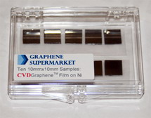
Multilayer Graphene Film on Nickel, Ten 10mmx10mm samples |
Multilayer Graphene Film on Nickel |
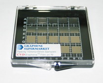
| Multilayer Graphene Film on Nickel, Twenty 10mmx10mm samples |
| Multilayer Graphene Film on NickelȘOne Wafer 100mm (4 in) |
| ëÙýÙ£ªçËýÐò₤á¨üˋ |
Single Layer Graphene on Copper foil: 2"x2" |
Copper foil thickness: 20 micron |
| Single Layer Graphene on Copper foil: 4"x2" |
| Single Layer Graphene on Copper foil: 4"x4" |
| ÀÀ |
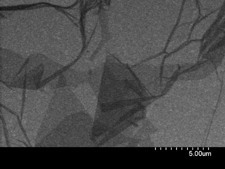
| CVDò₤á¨üˋTEM grids |
25 pack: CVDGraphene TEM Grid on Copper 2000 support |
CVD Graphene film deposited on ultrafine copper TEM grids, 2000 Mesh
Use CVD graphene grown on Ni to prepare TEM grids
Thickness of CVD Graphene film: 0.3-2 nm (1-6 monolayers)
Typical graphene coverage:60-90% |
| 5 pack: CVDGraphene TEM Grid on Copper 2000 support |
| 25 pack: CVDGraphene TEM Grid on Lacey Carbon Support |
CVD Graphene film deposited on Lacey carbon TEM grids, 300 Mesh
Use CVD graphene grown on Ni to prepare TEM grids
Thickness of CVD Graphene film: 0.3-2 nm (1-6 monolayers)
Typical graphene coverage:60-90% |
| 5 pack: CVDGraphene TEM Grid on Lacey Carbon Support |
| Trial pack: 10 CVDGraphene TEM Grids 5/5 |
5 CVD Graphene film deposited on lacey carbon TEM grids (300 Mesh) and 5 CVD Graphene film deposited on Copper TEM grids (2000 Mesh).
Use CVD graphene grown on Ni to prepare TEM grids
Thickness of CVD Graphene film: 0.3-2 nm (1-6 monolayers)
Typical graphene coverage:60-90% |
| ÀÀ |
| êÂäÍÑÁýÐò₤á¨üˋ |
3D Multilayer Graphene Film on Nickel Foam, 2"x2" |
3D Multilayer graphene on Ni Foam |
| 3D Multilayer Graphene Film on Nickel Foam, 2"x4" |
| 3D Monolayer Graphene Film on Copper Foam, 1.5"x1.5", TWO Pack |
3D graphene on Cu Foam |
| 3D Monolayer Graphene Film on Copper Foam, 2"x4" |
| ÀÀ |
| ò₤á¨üˋáèûæñÜáˋ |
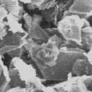
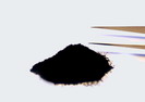
Graphene Nanopowder: 3 nm Flakes - 1 g |
Grade AO-1 dry black powder
Specifications:
Specific surface area-600 m2/g
Color: Black
Solid content: 98%
Carbon: 97%, Hydrogen 1%, Oxygen 2%
Average flake thickness: 1 nm (less than 3 monolayers)
Average Particle (lateral) size: ~10 microns. |
| Graphene Nanopowder: 3 nm Flakes-Trial Size 0.5 g |
| Graphene Nanopowder: 8 nm Flakes- 5 g |
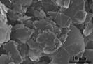
Grade AO-2 dry powder
Specific surface area-100 m/g2
Color: Black
Purity: 99.9%
Average flake thickness: 8 nm (20-30 monolayers)
Average Particle (lateral) size: ~ 550 nm (150-3000) nm.? |
| Graphene Nanopowder: 8 nm Flakes- 25 g |
| Graphene Nanopowder: 12 nm Flakes-5 g |
Grade AO-3 dry powder
Specifications:
Specific surface area-80 m/g2
Color: Black
Purity: 99.2%
Average flake thickness: 12 nm (30-50 monolayers)
Average Particle (lateral) size: ~ 4500 nm (1500-10000) nm. |
| Graphene Nanopowder: 12 nm Flakes-25 g |
| Graphene Nanopowder: 12 nm Flakes-100 g |
| Graphene Nanopowder: 60 nm Flakes- 25 g |
Grade AO-4 dry powder
Specifications:
Specific surface area<15 m/g2
Color: Black
Purity: 98.5%
Average flake thickness: 60 nm
Particle (lateral) size: ~ 3-7 microns. |
| Graphene Nanopowder: 60 nm Flakes-100 g |
| Graphene Nanopowder: Grade C1, 25 g |
Grade C1
Specifications:
Specific surface area-60 m/g2
Color: Black
Purity: 97%
Average flake thickness: 5-30nm
Average Particle (lateral) size: ~ 5-25 microns. |
| Graphene Nanopowder: Multilayer flakes, 5 g? |
Grade MO-1
Specifications:
Specific surface area-60 m/g2
Color: Black
Purity: 99.9%
Average flake thickness: 28 nm
Density: 2 g/cm3 |
| Graphene Nanopowder: Multilayer flakes, 25 g |
| Graphene Nanopowder Trial kit |
Graphene Nanopowder Grade AO-2, 1 g
Graphene Nanopowder Grade AO-3, 5 g
Graphene Nanopowder Grade AO-4, 5 g
Graphene Nanopowder Grade C-1, 5 g |
| çËýÐò₤á¨üˋàÉؤ |
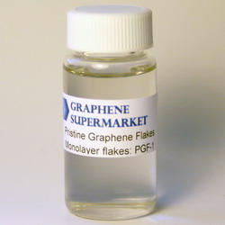
Pristine Graphene Monolayer Flakes (50 ml) |
Dispersion in ethanol.
Concentration: 1 mg/L
Carbon content: 99.99%
Ultrapure: no oxidation, no surfactants
Average flake thickness: 0.35 nm (1 monolayer)
Average Particle (lateral) size: ~ 550 nm (150-3000) nm. |
| Ǩç¥ò₤á¨ø§ |
Conductive Graphene Paper |
Diameter of Graphene Film: 100 mm
Average thickness: 45 microns
Electrical Conductivity: about 1000 S/cm
Silvery/Nontransparent |
| ÀÀ |
| çËýÐî¾£₤ò₤á¨üˋ |
Single Layer Graphene Oxide: 100 mg |
Dry powder
Color:Brown
Composition: Carbon (79%), Oxygen (20%)
Flake size: 0.5-5 microns.
Thickness: 1 atomic layer - at least 80%.
Graphene oxide disperses readily in water and other solvents, breaking up into macroscopic flakes, mostly one layer thick. Graphene oxide layers are about 1.1 Àâ 0.2 nm thick. |
| Single Layer Graphene Oxide: 500 mg |
| High Porosity Reduced Graphene Oxide-250mg |
dry black powder
Specific surface area-about 400 m2/g
Color: Black
Solid content: 98%
Average flake thickness:1 monolayer
Average Particle (lateral) size: ~3-10 microns.
Flakes have multiple openings and holes
Improved solubility in organic solvents? |
| High Porosity Reduced Graphene Oxide-500mg |
| High Surface Area Reduced Graphene Oxide 75 mg |
dry black powder
Specifications:
Specific surface area-833 m2/g
Color: Black
Solid content: 98%
Carbon/Oxygen Ratio 10.5
Average flake thickness:1 monolayer
Average Particle (lateral) size: ~3-5 microns. |
| î¾£₤ò₤á¨üˋ |
Reduced Graphene Oxide: 60 mg, Dry Nanopowder |
Color: Black
Single layer flakes >50%
Low concentration of lattice defects
Specific surface area (SSA) >250m2/g
Lateral size: 1um-10um
Thickness: 0.5-0.6 nm |
| çËýÐî¾£₤ò₤á¨üˋùÛàÉؤ |
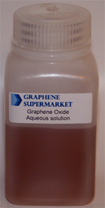
Single Layer Graphene Oxide Dispersion in Water: 60 ml |
Aqueous dispersion, 60 ml
Concentration: 275 mg/L
Composition: Carbon (79%), Oxygen (20%)
Flake size: 0.5-5 microns.
Thickness: 1 atomic layer - at least 80%.
Color:Brown |
| Single Layer Graphene Oxide Dispersion in Water: 175 ml |
| Highly Concentrated Single Layer Graphene Oxide Dispersion in Water:60 ml |
Concentration: 5g/L, 0.33g per bottle
Composition: Carbon (79%), Oxygen (20%)
Flake size: 0.5-0.7 microns.
Thickness: 1 atomic layer - at least 60%.
Color:Brown |
| Highly Concentrated Single Layer Graphene Oxide Dispersion in Water:175 ml |
| Highly Concentrated Single Layer Graphene Oxide Dispersion in Water:1000 ml |
| ýÈêÏ£ªî¾£₤ò₤á¨üˋ |
The Graphene OxideThin Film on Glass |
Diameter of Graphene Oxide Film: 35 mm
Thickness: 175 nm
Deposited on a round slide: D=50.8 cm, thickness=1 mm |
| î¾£₤ò₤á¨üˋø§ |
Graphene Oxide Paper |
Diameter:4.0cm
Thickness: 10 microns
Non-conductive
Tensile modulus> 20 GPa
Color: Black
Bends easily |
|
| Kishò₤á¨üˋ |
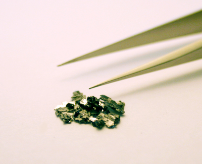
Natural Kish Graphite (Grade 200), 5g |
Ultrapure: Carbon>99.2%, Moisture<0.35%
Flake size: 0.7-2 mm |
| Natural Kish Graphite (Grade 300), 0.2g |
Ultrapure: Carbon>99%
Large Flakes: size 1-3 mm |
| Natural Kish Graphite (Grade 300), 0.5g |
|
| ò₤á¨üˋæˆØó |
5 Pack: Graphene Transfer Tape |
Thermal Release Tape, 5 pack
Size: 200 mm x 200 mm |
| Graphene Transfer Kit |
Twographene release Tapes (Size: 200 mm x 200 mm)
Single Layer Graphene on Copper foil: 2"x2"
Trial pack: Twenty 10mmx10mm samples, Graphene Film on Nickel |

 üÔíµCCD¿ãüù¿ãóæØú