石墨烯转移,石墨烯套装,基CVD石墨烯TEM网格,铝膜基石墨烯,单层石墨烯溶液,石墨烯纳米星 |
 |
石墨烯
Graphene
Graphene Transfer Tape,
石墨烯转移胶带
Graphene Transfer Kit,
石墨烯转移套装
Graphene Film Trial Kit,
石墨烯膜套装
Graphene Nanopowder Trial kit,
石墨烯纳米粉末套装
Graphene Transfer Kit,
石墨烯转移套装
Graphene Kit: Beginner's Value Package,
石墨烯套装
Graphene Kit: Scotch Tape Value Package,石墨烯套装
CVD Graphene TEM Grid on Copper 2000 support,铜基CVD石墨烯TEM网格
CVD Graphene TEM Grid on Lacey Carbon Support,
碳基CVD石墨烯TEM网格
Trial pack 10 CVD Graphene TEM Grids,
CVD石墨烯TEM网格套装
Graphene on Aluminum Foil,铝膜基石墨烯
Pristine Graphene Monolayer Flakes,单层石墨烯溶液
Graphene Nano-Stars,石墨烯纳米星
石墨烯转移 Graphene Transfer |
|||
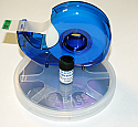
| Graphene Transfer Tape 石墨烯转移胶带 |
5 Pack |  |
Thermal Release Tape, 5 pack Specifications: Size: 200 mm x 200 mm One-sided 100oC release temperature The procedure for transferring graphene with the thermal release tape is simple; however, it is difficult to obtain continuous coverage. If continuous coverage is not a requirement, graphene transfer using our thermal release tape may be the best option for you. Using thermal release tape, the residue is low; however, there is only about 70% coverage and the graphene is not continuous. Using PMMA, there may be mild contamination, but it is high-quality, continuous graphene, at 99% coverage. If you require complete continuous coverage, we strongly recommend purchasing graphene on substrates transferred using the PMMA method at our laboratory. |
| Graphene Transfer Kit 石墨烯转移套装 |
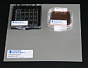 |
Graphene Transfer Kit includes: Two graphene release Tapes (Size: 200 mm x 200 mm) Single Layer Graphene on Copper foil: 2"x2" Trial pack: Twenty 10mmx10mm samples, Graphene Film on Nickel Specifications of transfer tape: Size: 200 mm x 200 mm One-sided 100oC release temperature The procedure for transferring graphene with the thermal release tape is simple; however, it is difficult to obtain continuous coverage. If continuous coverage is not a requirement, graphene transfer using our thermal release tape may be the best option for you. Using thermal release tape, the residue is low; however, there is only about 70% coverage and the graphene is not continuous. Using PMMA, there may be mild contamination, but it is high-quality, continuous graphene, at 99% coverage. If you require complete continuous coverage, we strongly recommend purchasing graphene on substrates transferred using the PMMA method at our laboratory. |
|
石墨烯套装 Graphene Value Kits |
|||
| Graphene Film Trial Kit 石墨烯膜套装 |
 |
Includes: Two Single/Double Layer Graphene samples on 285 nm Silicon Dioxide Wafers: 1cm x 1 cm Two 10mmx10mm samples, Graphene Film on Nickel: 1 cm x 1 cm One sample of Multilayer Graphene on a 285 nm Silicon Dioxide Wafer: 1 cm x 1 cm One sample of Monolayer Graphene on a 285 nm Silicon Dioxide Wafer: 1 cm x 1 cm One sample of Monolayer Graphene on Glass: 1" x 1" If you are interested in investigating numerous different samples of graphene coatings, this trial kit is ideal. All of the samples are made by Chemical Vapor Deposition and give a strong Raman signal. A great value for students and scientific researchers alike interested in trying different samples. |
|
| Graphene Nanopowder Trial kit 石墨烯纳米粉末套装 |
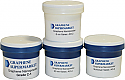 |
Includes: Graphene Nanopowder Grade AO-2, 1 g Graphene Nanopowder Grade AO-3, 5 g Graphene Nanopowder Grade AO-4, 5 g Graphene Nanopowder Grade C-1, 5 g |
|
| Graphene Kit: Beginner's Value Package 石墨烯套装 |
 |
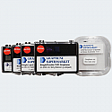
Perfect for students and teachers. This kit may be used to exfoliate graphene using the "scotch tape method." The material may also be deposited onto the wafers to examine under Raman. Please note that you will not be able to create continuous films using this kit, it is for educational purposes. If you require continuous graphene films, consider our Graphene Film Trial Kit Graphene Kit includes: Kish Graphite (grade 200): 1 gram. Graphene Oxide (Aqueous Dispersion): 25 ml Pristine graphene in solution: 25 ml. Eight small Silicon/ 300 nm Silicon Dioxide wafers: 10 mmx10 mm squares. Graphene Scotch tape: 1 roll. |
|
| Graphene Kit: Scotch Tape Value Package 石墨烯套装 |
 |
Graphene Kit includes: Our Premium Kish Graphite (grade 300): 0.2 gram. One Silicon/ 285 nm Silicon Dioxide wafer: 4" Diameter Graphene Scotch tape: 1 roll. |
|
石墨烯TEM网格 Graphene TEM grids |
|||
| CVD Graphene TEM Grid on Copper 2000 support 铜基CVD石墨烯TEM网格 |
5 pack | 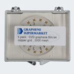 |
CVD Graphene film deposited on Copper TEM grids (2000 Mesh) We use CVD graphene grown on Ni to prepare TEM grids Thickness of CVD Graphene film: 0.3-2 nm (1-6 monolayers) Typical graphene coverage:60-90% Ultrathin CVD Graphene grids provide the ideal specimen support to achieve high resolution data in TEM imaging making them an ideal choice many TEM applications. |
| 25 pack | 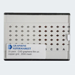 |
||
| CVD Graphene TEM Grid on Lacey Carbon Support 碳基CVD石墨烯TEM网格 |
5 pack | 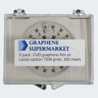 |
CVD Graphene film deposited on lacey carbon TEM grids, 300 Mesh. We use CVD graphene grown on Ni to prepare TEM grids Thickness of CVD Graphene film: 0.3-2 nm (1-6 monolayers) Typical graphene coverage:60-90% Ultrathin CVD Graphene grids provide the ideal specimen support to achieve high resolution data in TEM imaging making them an ideal choice many TEM applications. |
| 25 pack | 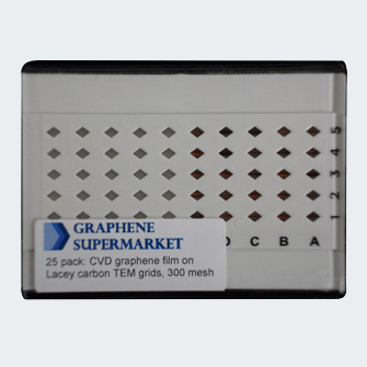 |
||
| Trial pack 10 CVD Graphene TEM Grids CVD石墨烯TEM网格套装 |
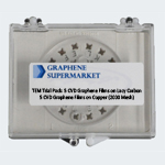 |
Trial pack: 10 CVD Graphene TEM grids includes: 5 CVD Graphene film deposited on lacey carbon TEM grids (300 Mesh) and 5 CVD Graphene film deposited on Copper TEM grids (2000 Mesh). We use CVD graphene grown on Ni to prepare TEM grids Thickness of CVD Graphene film: 0.3-2 nm (1-6 monolayers) Typical graphene coverage:60-90% Ultrathin CVD Graphene grids provide the ideal specimen support to achieve high resolution data in TEM imaging making them an ideal choice many TEM applications. |
|
石墨烯膜 Graphene Coatings |
|||
| Graphene on Aluminum Foil 铝膜基石墨烯 |
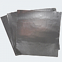 |
Aluminium foil coated with graphene nanoplatelets 9"x8.5" 5 Sheets Properties of graphene coating: Average Thickness: 3.5nm Lateral Size of individual graphene flakes: 5-10μm The flakes coat the surface to form a conductive layer Properties of aluminum foil: Thickness: 16μm Electrical Resistivity- 4.5x10⁻⁶ Ω.cm In the lithium ion battery industry -- which includes mobile phones, notebooks, hybrid electric vehicles, etc -- aluminium foil coated with graphite, carbon black, or carbon nanotubes is used as a positive electrode's electron collector. When coated with graphene, the aluminium foil has significantly improved electrical resistivity; aluminum foil coated with graphene is 4.5x10⁻⁶ Ω.cm, whereas foil coated with carbon black is 7x10⁻⁶ Ω.cm. This product may be supplied on a roll - 0.5m width, up to 2000m length SEM图像1 / SEM图像2 / 拉曼光谱图 / 图片 |
|
石墨烯溶液 Graphene Solutions |
|||
| Pristine Graphene Monolayer Flakes 单层石墨烯溶液 |
50 ml | 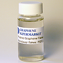 |
Dispersion in ethanol. Concentration: 1 mg/L Carbon content: 99.99% Ultrapure: no oxidation, no surfactants Average flake thickness: 0.35 nm (1 monolayer) Average Particle (lateral) size: ~ 550 nm (150-3000) nm. |
石墨烯纳米星 Graphene Nano-Stars |
|||
| Graphene Nano-Stars 石墨烯纳米星 |
0.25 g |  |
Graphene Nano-Stars are made of graphene sheets which are wrapped and form cone shapes. One end of the cone is capped similar to a fullerene. Each cone is 30-50 nm in length and 2-5 nm in diameter. These cones tend to group together and form a cluster which can be characterized as nano-stars. Graphene Nano-Stars have many of the same properties as graphene – high electrical and thermal conductivity, as well as ease of functionalization. Properties: Diameter: 3-5 nm Length: 30-50 nm Cluster diameter: 60-120 nm Density: 1.1 g/cm3 Bulk density: >15 g/dm3 Active surface: 250 m2/g SEM图像 / TEM图像1 / TEM图像2 |
|
上海玻色智能科技有限公司 上海: (021)3353-0926, 3353-0928 北京: (010)8217-0506 广州: 139-0221-4841 武汉: 139-1733-4172 全国销售服务热线:4006-171751 Email: info@bosontech.com.cn www.BosonTech.com.cn 2008-2022 All Rights Reserved! |
|